
Your shopping cart is empty!
Categories
- 3D Printing and Plastic peripherals (8)
- 433Mhz and Lora (9)
-
Amateur Radio (623)
- - Antenna Analyzer (10)
- - APRS (11)
- - ATU (3)
- - CW (1)
- - Digital Modes (9)
- - DMR (4)
- - Echolink (9)
- - Enclosure (13)
- - Eshail-2 (QO-100) (66)
- - GPS (6)
- - iGate (1)
- - Microcontrollers (44)
- - Microphone (1)
- - Power Supply (6)
- - Programming Cable (5)
- - QRP (8)
- - Radio interface (19)
- - Receiver (7)
- - Repeater (4)
- - RF Amplifiers (21)
- - RF Kits (18)
- - RF modules (114)
- - Rotator (1)
- - SDR (71)
- - Spectrum Analyzer (4)
- - SWR (9)
- - Transceiver (57)
- - WSPR (5)
- Antennas and Acc (312)
- Audio and Video (28)
- Bargain Box (1)
- Battery (3)
- Bluetooth (11)
- Cables (35)
- Computer Peripherals (103)
- Connectors (82)
- Data acquisition (1)
- Display (1)
- Electromechanical (25)
- Enclosure (12)
- GPS (5)
- Hardware (1)
- Home Automation (127)
- Inverter (9)
- Liquid (7)
- Lora (8)
- Microcontrollers (119)
- Modbus (3)
- MQTT (14)
- Network Radio (3)
- Networking (8)
- Power (133)
- Power supply (48)
- Radio Interface (14)
- RF Modules (139)
- ROIP (2)
- Satellite (90)
- Security (13)
- Sensor (16)
- Solar (14)
- Test and Measurements (61)
- Tools and Equipment (7)
- VOIP (9)
- Weather (1)
DC 2.3V-5.5V Frequency 0-12.5MHZ AD9833 DDS Signal Generator Module Triangle Sine Wave Signal Source Programmable Microprocessors Module

Price: R197.00
Ex Tax: R197.00
Ex Tax: R197.00
Qty:
- OR -
Add to Wish List
Add to Compare
Add to Compare

DC 2.3V-5.5V Frequency 0-12.5MHZ AD9833 DDS Signal Generator Module Triangle Sine Wave Signal Source Programmable Microprocessors Module
AD9833 is a programmable waveform generator capable of generating a frequency 0-12.5MHZ sine, triangle, square wave signal. Waveform generator is widely used in a variety of measurement, excitation and time domain response field, output frequency and phase are programmable via software, easy to adjust, clocked clock is 25MHz, precision 0.1Hz, clock frequency is 1MHz, the precision You can reach 0.004Hz. Via three serial interfaces to write data.
Application:
- Frequency excitation / waveform generation. Liquid, gas flow measurement.
- Sensing applications - approximation, sports, defect detection.
- Linear loss, linear decay.
- Test equipment, medical equipment
- Scan clock generator
Module Features:
1, Working voltage: 2.3V-5.5V.
2, Working temperature range: -40 ~ + 105 prefix = o
3, Onboard 25MHZ (accuracy of 50ppm) active crystal, stepping accuracy 0.1HZ.
4, On-board high-speed amplifiers 300M and also has a low-pass filtering.
5, Two-channel output signal, an original signal output, an amplified output signal 5 times, 50Ohm output impedance.
6, Size: 32mm X 32mm.
7, Support universal plate (tunnel plate), a multiple-board pins are 2.54mm, can be easily solderd as an universal board.
The package include:1 sets
Software lib MD_AD9833
Device Control with Arduino
Library for using a AD9833 Programmable Waveform Generator.
The AD9833 is a low power, programmable DDS waveform generator capable of producing sine, triangular, and square wave outputs. The library provides access to all on-chip features.
AD9833 Operation
The AD9833 communicates with microcontrollers via SPI. It has a control register for its configuration and frequency and phase registers for specifying the frequency and phase of the output waveform.
Note that there are two channels, thus, there is one frequency and phase registers for each channel. The frequency output is calculated by using the formula:
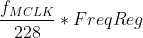
Where fMCLK is equal to the crystal frequency on MCLK pin. This output frequency is then shifted to a phase given by:
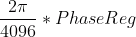
FreqReg (28-bit) and PhaseReg (12-bit) are data to be written to the frequency and phase registers.
Understanding phase and frequency in waveforms.
Control and Data Bits
For the AD9833 to operate, the microcontroller sends 16-bit words in frames. The state of the FSYNC pin acts as a frame for each 16-bit word, that is, the AD9833 can only read data when FSYNC is low.
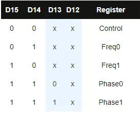
Bits 15 and 14 determine the location of the register to which the data is written to. When these bits are both 0, data is sent to the control register. Otherwise, data is sent to other registers. See table below:
The rest of the bits are either data (when in frequency or phase write) or other control bits.
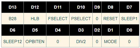
When writing to the control register, the rest of the bits are as follows:
B28 - if set, allows two successive frames as 14 MSBs and 14 LSBS.
HLB - if B28 is not set, the state of HLB determines if the received data is 14 MSB (HLB=1) or 14 LSB (HLB=0).
FSELECT - determines which channel to use for frequency
PSELECT - determines which channel to use for phase
RESET - resets internal registers but not the frequency, phase and control registers
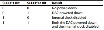
SLEEP1, SLEEP12
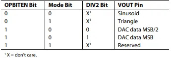
OPBITEN, DIV2, MODE
You cannot configure the AD9833 with just a single 16-bit word. A series of frames must be sent by the microcontroller to achieve the right configuration.
Example Data Transmission
Let’s have an example: a 25 MHz crystal attaches to the MCLK pin and your target is a 400 Hz sine wave at channel 0, without any phase shift. The value to be written to the frequency register is then:

The first 16-bit word to be sent is for the control register. We also want the IC to reset. Hence, the 16 bits would be:
![]()
Note that bit 13 (B28) is set because we want that successive frames be written immediately to the frequency register. Also notice that the OPBITEN, Mode and DIV2 bits are also zeroes, indicating that the output waveform is a sine wave.
The next word would be:
![]()
Here, bit 15 and 14 points to the Freq0 register address (channel 0). The rest of the bits is the 14 MSB of the frequency we calculated earlier.
The next word:
![]()
Still, bits 15 and 14 points to Freq0 and the rest of the bits are the 14 LSB of the frequency, which is now all zeroes.
Next we write to the phase register, even though it’s zero in this case:
![]()
Here, bits 15 and 14 points to Phase0.
Finally, we have:
![]()
This writes to control register and issues a reset. A signal then appears at the output after seven MCLK cycles.
Using the AD9833 with Arduino
Exsample code avalable here MD_AD9833_Basic.ino
Compatibility
This library is compatible with all architectures so you should be able to use it on all the Arduino boards.
To use this library, open the Library Manager in the Arduino IDE and install it from there.
- 1.2.2 (latest)
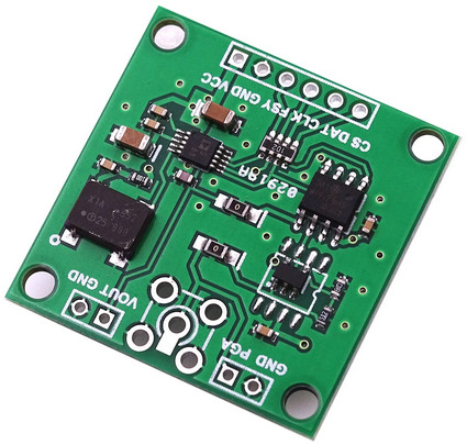
Breakout Module connector
| Module pin | Description |
| CS | SPI Chip select to MCP41010 |
| DAT | SPI MOSI to AD9833 and MCP41010 |
| CLK | SPI Clock to AD9833 and MCP41010 |
| FSY | SPI Chip select for AD9833 |
| GND | 0V |
| VCC | 3V ~ 5V |
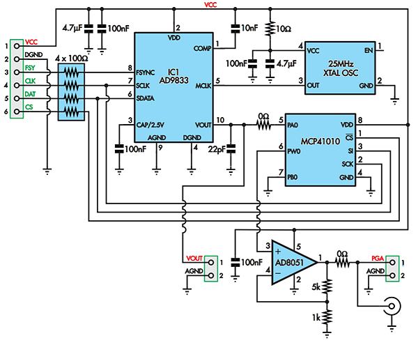
Circuit Connections
For the AD9833 make the following connections from an Arduino Uno to the breakout board:
DAT 11 /// SPI Data pin number
CLK 13 /// SPI Clock pin number
FSY 10 /// chip select (FSYNC in AD9833 usage)
Additionally for the MCP41010 make the following connection:
CS 9 /// chip select for MCP41010
10Mhz Signal Generator code below
#include <SPI.h>
#include <MD_AD9833.h>
// Pins for SPI comm with the AD9833 IC
#define DATA 11 ///< SPI Data pin number
#define CLK 13 ///< SPI Clock pin number
#define FSYNC 10 ///< SPI Load pin number (FSYNC in AD9833 usage)
#define CS_DIGIPOT 9 // MCP41010 chip select - digital potentiometer.
MD_AD9833 AD(FSYNC); // Hardware SPI
//MD_AD9833 AD(DATA, CLK, FSYNC); // Arbitrary SPI pins
// Character constants for commands
const char CMD_HELP = '?';
const char BLANK = ' ';
const char PACKET_START = ':';
const char PACKET_END = ';';
const char CMD_FREQ = 'F';
const char CMD_PHASE = 'P';
const char CMD_OUTPUT = 'O';
const char OPT_FREQ = 'F';
const char OPT_PHASE = 'P';
const char OPT_SIGNAL = 'S';
const char OPT_1 = '1';
const char OPT_2 = '2';
const char OPT_MODULATE = 'M';
const uint8_t PACKET_SIZE = 20;
void setup()
{
pinMode(CS_DIGIPOT,OUTPUT);
Serial.begin(57600);
AD.begin();
usage();
// take the CS pin low to select the chip:
digitalWrite(CS_DIGIPOT,LOW);
// send in the address and value via SPI:
SPI.transfer(B00010001);
// write out the value
SPI.transfer(127);
// take the CS pin high to de-select the chip:
digitalWrite(CS_DIGIPOT,HIGH);
}
void usage(void)
{
Serial.print(F("\n\n[MD_AD9833_Tester]"));
Serial.print(F("\n?\thelp - this message"));
Serial.print(F("\n\n:<cmd><opt> <param>;"));
Serial.print(F("\n:f1n;\tset frequency 1 to n Hz"));
Serial.print(F("\n:f2n;\tset frequency 2 to n Hz"));
Serial.print(F("\n:fmn;\tset frequency modulation to n Hz"));
Serial.print(F("\n:p1n;\tset phase 1 to n in tenths of a degree (1201 is 120.1 deg)"));
Serial.print(F("\n:p2n;\tset phase 2 to n in tenths of a degree (1201 is 120.1 deg)"));
Serial.print(F("\n:ofn;\toutput frequency n or modulation [n=1/2/m]"));
Serial.print(F("\n:opn;\toutput phase n or modulation [n=1/2/m]"));
Serial.print(F("\n:osn;\toutput signal type n [n=(o)ff/(s)ine/(t)riangle/s(q)uare]"));
}
uint8_t htoi(char c)
{
c = toupper(c);
if (c >= '0' && c <= '9')
return(c - '0');
else if (c >= 'A' && c <= 'F')
return(c - 'A' + 10);
else
return(0);
}
char nextChar(void)
// Read the next character from the serial input stream
// Blocking wait
{
while (!Serial.available())
; /* do nothing */
return(toupper(Serial.read()));
}
char *readPacket(void)
// read a packet and return the
{
static enum { S_IDLE, S_READ_CMD, S_READ_MOD, S_READ_PKT } state = S_IDLE;
static char cBuf[PACKET_SIZE + 1];
static char *cp;
char c;
switch (state)
{
case S_IDLE: // waiting for packet start
c = nextChar();
if (c == CMD_HELP)
{
usage();
break;
}
if (c == PACKET_START)
{
cp = cBuf;
state = S_READ_CMD;
}
break;
case S_READ_CMD: // waiting for command char
c = nextChar();
if (c == CMD_FREQ || c == CMD_PHASE || c == CMD_OUTPUT)
{
*cp++ = c;
state = S_READ_MOD;
}
else
state = S_IDLE;
break;
case S_READ_MOD: // Waiting for command modifier
c = nextChar();
if (c == OPT_FREQ || c == OPT_PHASE || c == OPT_SIGNAL ||
c == OPT_1 || c == OPT_2 || c == OPT_MODULATE)
{
*cp++ = c;
state = S_READ_PKT;
Write a review
Your Name:Your Review: Note: HTML is not translated!
Rating: Bad Good
Enter the code in the box below:


Powered By OpenCart
Giga Technology © 2024
Giga Technology © 2024